LITHOSCALE ®
LITHOSCALE
Maskless Exposure Lithography System。is a revolutionary, highly versatile maskless exposure lithography platform geared for a variety of microfabrication applications accommodatin
广西科米瑞实验仪器设备有限公司提供 EV Group LITHOSCALE 产品资料、选型咨询、供货报价和售后服务支持,价格面议。
← 返回产品列表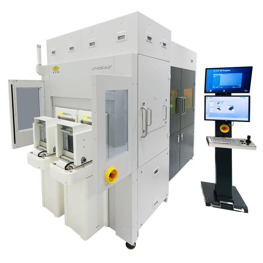
说明
Maskless Exposure Lithography System
LITHOSCALE ® is a revolutionary, highly versatile maskless exposure lithography platform geared for a variety of microfabrication applications accommodating wafers up to 300 mm.
The LITHOSCALE system featuring EV Group’s MLE™ maskless exposure technology tackles legacy bottlenecks by combining powerful digital processing that enables real-time data transfer and immediate exposure, high structuring resolution and throughput scalability. Its mask-free approach eliminates mask-related consumables, while the exposure system with its tunable solid-state laser source is designed for high redundancy and long life-time stability with unique auto-calibration capabilities that minimize maintenance. Powerful real-time digital processing enables immediate exposure from the design-file to the substrate – thereby avoiding hours of conversion time for each digital mask layout. LITHOSCALE features high-resolution (<2µm L/S), dynamically die-level addressable exposure of the entire substrate surface, which enables agile consumable-free processing and low cost of ownership (CoO). The LITHOSCALE system integrates full-wafer top-and-backside alignment utilizing dedicated objectives with visible and IR capability and proprietary chuck designs accommodating wafer sizes up to 300 mm. The system features dynamic alignment modes with an automatic focus, in order to adapt to the substrate material and surface variations. The ability to finely control focus level position keeps sidewalls steep as well as desired 3D contour of the resist, while preventing edge topping and footing. Large working distance and automatic adaptive focus ensures patterning uniformity across the exposure surface. It also offers individualized die processing capability, while fast full-field positioning and dynamic alignment enable high scalability for a range of substrate sizes and shapes.
Features
Wafer/substrate size up to 300 mm/12’’
Resolution capability < 2 µm L/S
Equipped with MLE technology featuring high-end diffraction-limited optics
Exposure spectrum of 375-nm and/or 405-nm wavelength; user definable either as single, broadband or any kind of wavelength mixture
Regularly monitored and auto-calibrated solid-state light source securing its long-life-time stability and high redundancy
Advanced alignment modes supporting multi-point alignment, top-side and bottom-side VIS and IR alignment capability
Depth of focus control (DoF) < 24 µm
Adaptive autofocus control (AF) < 100 µm
High-precision, fast full-field positioning and field proven alignment stage embedding high-tech mechatronics and calibration sensors for entire system stability
Advanced software features including: Dynamic die-level annotation Advanced distortion compensation Mask-file transfer and recipe execution via host/flexible per each wafer Layout transformation function Alternative format files support: Gerber, ODB++, OASIS
Dynamic die-level annotation
Advanced distortion compensation
Mask-file transfer and recipe execution via host/flexible per each wafer
Layout transformation function
提交需求
请填写必填信息,我们将在工作日尽快回复。