LITHOSCALE ® XT
LITHOSCALE XT
High Throughput Maskless Exposure Lithography System。is a revolutionary, highly versatile maskless exposure lithography platform geared for a variety of microfabrication applicati
广西科米瑞实验仪器设备有限公司提供 EV Group LITHOSCALE XT 产品资料、选型咨询、供货报价和售后服务支持,价格面议。
← 返回产品列表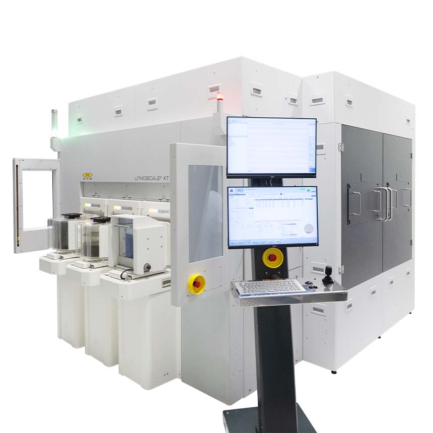
说明
High Throughput Maskless Exposure Lithography System
LITHOSCALE ® XT is a revolutionary, highly versatile maskless exposure lithography platform geared for a variety of microfabrication applications accommodating wafers up to 300 mm.
EVG’s LITHOSCALE® XT provides up to a five-fold increase in throughput versus the previous industry benchmark LITHOSCALE® system, supporting 300mm wafers and 300mm square substrates. The system is ideally suited for applications involving multi-die patterning, fan-out wafer-level packaging (FoWLP) for AI and high-performance computing (HPC) devices, panel-level packaging (PLP), MEMS, advanced imaging sensors, and die traceability for security and automotive applications. The LITHOSCALE® XT processing pipeline digitally transforms vectorized pattern data and compensates for distortions during exposure based on pre-measured and real-time acquired alignment information.
Operating at single or, simultaneously, at two wavelength bands (λ≈375 and 405 nm), thin & thick resists, dielectric materials, transparent, black, RGB or IR resists as well as many other established and novel materials are optimally exposed. An individual ‘exposure matrix’ permits to select arbitrary pairs of test parameters, such as exposure dose, spectral composition focal position, and exposure speed, to quickly determine the optimum process recipe and multi-dimensional process windows during the production ramp–up phase, thereby minimizing set-up times and simplifying material changes. This equipment allows for excellent process control, including sidewall profile, complex topography structure and high aspect ratio patterning. Exposure is performed on the full wafer surface, demonstrating zero stitch performance.
The LITHOSCALE® XT is a prime example of a digital high-volume lithography system for advanced packaging applications. Its real-time auto focus, high depth of focus, dynamic distortion compensation, and broad process–matrix capabilities prove the benefits of the technology vs. traditional exposure systems for next-generation devices.
Features
Wafer sizes up to 300mm, panel size 300mm square
Six exposure heads with dual-stage concept
Dual wavelength, 375nm and 405nm, in one exposure head enabled by high-power UV laser diodes
High resolution, < 2 µm L/S
Full-wafer, zero-stitch patterning with no field–exposure or die-size limitations
Autofocus ±50 µm, Depth–of–focus ±12 µm, Working distance >6 mm
Topside, visible light, reflective IR alignment
Process and product compatibility with existing LITHOSCALE® product range
Real-time exposure layout correction for compensation of wafer-level distortion
Up to 16 alignment marks
Wafer layout formats: GDS II (standard), Gerber, OASIS, ODB++ (optional)
Supports a wide range of exposure applications: e.g., thin and thick photoresist (<1 micron up to >100 micron in thickness), chemically amplified resists, positive and negative tone, dielectrics, RGB and IR resist and high–aspect ratio patterning, etc
提交需求
请填写必填信息,我们将在工作日尽快回复。