LabRAM Odyssey Semiconductor
LabRAM Odyssey Semiconductor
LabRAM Odyssey Semiconductor microscope is the ideal tool for photoluminescence and Raman imaging on wafers up to 300 mm diameter, in order to fit both needs of wafer uniformity...
广西科米瑞实验仪器设备有限公司提供 HORIBA LabRAM Odyssey Semiconductor 产品资料、选型咨询、供货报价和售后服务支持,价格面议。
← 返回产品列表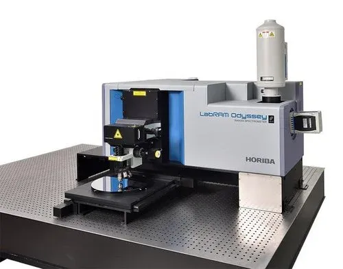
说明
产品说明
LabRAM Odyssey Semiconductor microscope is the ideal tool for photoluminescence and Raman imaging on wafers up to 300 mm diameter, in order to fit both needs of wafer uniformity assessment and defects inspection.
规格参数
| Dimensions | W × H × D (mm): 1400 × 620 × 1410 |
|---|---|
| Optical microscope | Open space microscope with white light reflection illumination, camera, 5×, 10×, 100× objectives as standard. Optional motorized objective turret. |
| Spectral range | Standard 200 nm - 2200 nm from sample to detector (achromatic, no change of optics required). |
| Imaging spectrometer | Focal length: 800 mm.Spectral resolution FWHM at 532 nm excitation wavelength ≤ 0.6 cm-1 with 1800 gr/mm and ≤ 0.3 cm-1 with 3000 gr/mm.Spectral stability RMS: < 0.02 cm-1 RMS Measured on Si 520 cm-1 line.Equipped with Open Electrode CCD (standard), optional EMCCD, optional InGaAs arrays detector (max. 3 detectors). |
| Spatial resolution | XY lateral resolution < 0.5 µm; Z axial resolution < 1.5 µm. |
| 300 mm × 300 mm motorized stage | XY high precision encoded motorized stage (X = 300 mm, Y = 300mm) with repeatability ≤1 µm; accuracy = 1 µm; resolution (encoder) = 50 nm; minimum motor step size = 10 nm. Z specifications: resolution (minimum step size) = 0.01 µm. Holders for 4" (100 mm), 6" (150 mm), 8" (200 mm) and 12" (300 mm) size wafers available. Vacuum compatible wafer holders. |
| Lasers | User selectable: 266 nm, 325 nm, 355 nm, 405 nm, 458 nm, 473 nm, 532 nm, 633 nm, 660 nm, 785 nm, & 1064 nm. Up to 6 motorized. |
| DuoScan™ | DuoScan™ technology for fast Laser scanning and Macrospot imaging (typical macrospot dimensions 30 µm × 30 µm with 50× objective). |
规格
| 型号/名称 | LabRAM Odyssey Semiconductor |
|---|---|
| 尺寸 | W × H × D (mm): 1400 × 620 × 1410 |
| Optical microscope | Open space microscope with white light reflection illumination, camera, 5×, 10×, 100× objectives as standard. Optional motorized objective turret. |
| Spectral range |
相关产品
提交需求
请填写必填信息,我们将在工作日尽快回复。