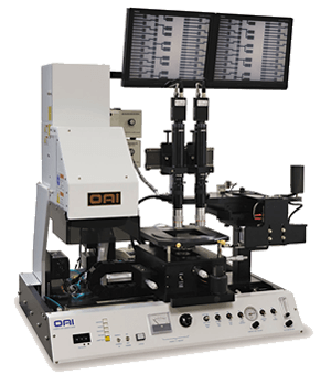
OAI 200E DUV Mask Aligner
Extreme DUV Mask Aligner 170nm-200nm。OAI’S Model 200E DUV Mask Aligner performs all the functions of the tabletop Model 200 Mask Aligner but utilizes a 185nm...
- 型号
- 200E DUV Mask Aligner
材料表征、热分析、力学、粒度、表面和物性测试设备
没有找到合适型号?
提交选型需求Extreme DUV Mask Aligner 170nm-200nm。OAI’S Model 200E DUV Mask Aligner performs all the functions of the tabletop Model 200 Mask Aligner but utilizes a 185nm...
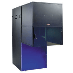
The OAI Model 30L Large Area UV Light Source is a large area collimated light source. The device is available with output power up to 10kW. Utilizing collima...
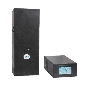
This UV LED light source is designed and engineered by the proven lithography experts at OAI. The light source delivers a number of unique benefits, the most...
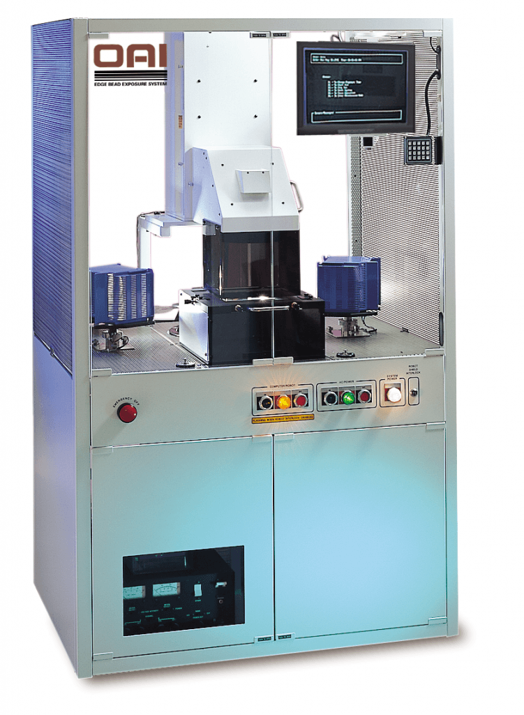
The OAI Model 2000 Exposure Systems may be configured as either an Edge-Bead Exposure System (2000SM) or a Flood Exposure System (2000AF); both configuration...
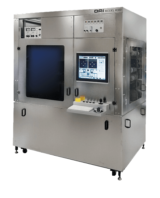
For Production Semiconductors, MEMS, Sensors, Advanced Packaging, IOT, Microfluidics
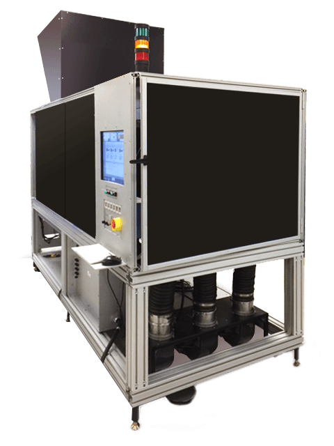
For Glass Panel Exposure。The Large Substrate Exposure System is designed for markets requiring exposure of large glass panels. Using OAI’s advanced beam opti...
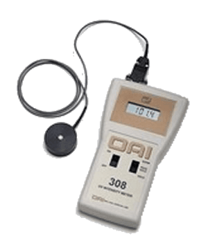
Dependable and repeatable, the OAI Model 308 UV Light Meter is a precise, direct-reading instrument designed to measure UV light intensity. The Model 308 fea...
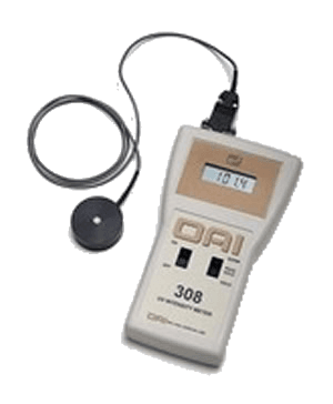
Built for high intensity applications, the OAI Model 308T UV Light Meter is a dependable, direct-reading instrument designed for measuring UV light intensity...
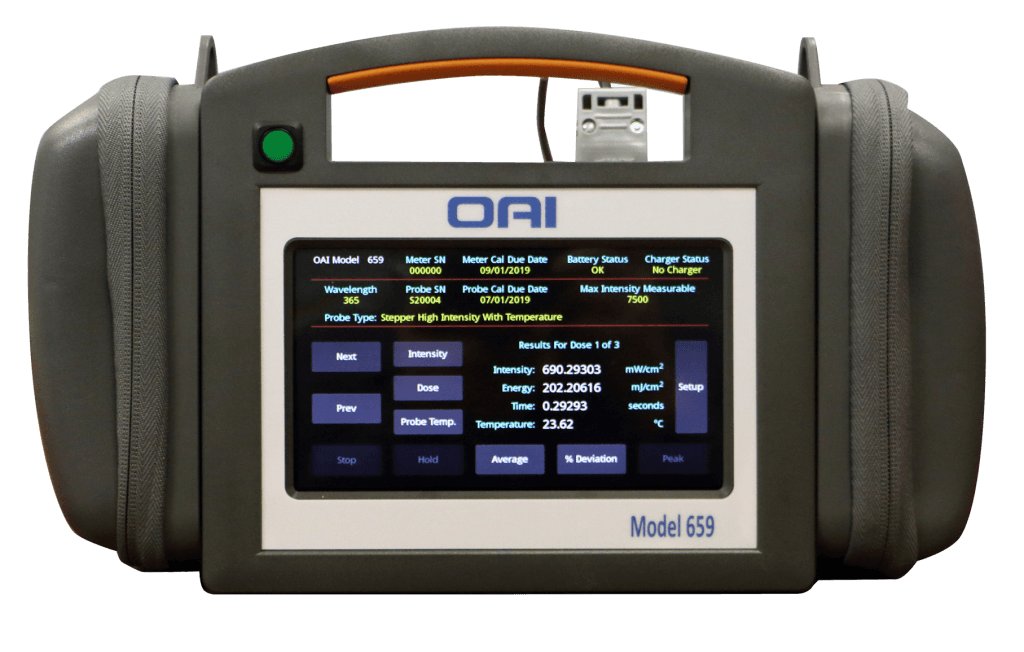
UV Light and Energy Meter for use with all wafer steppers Datasheet
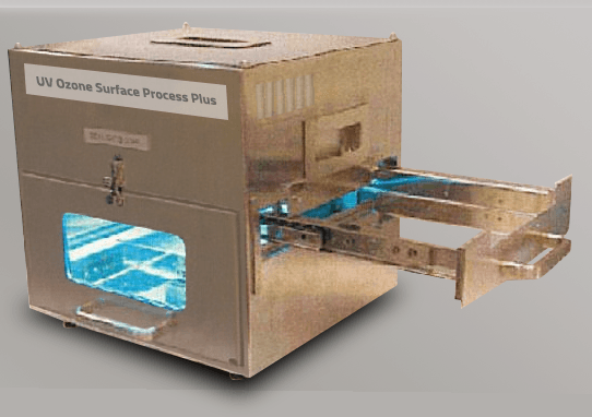
UV Ozone Treatment System Plus improves surface adhesion.。■ UV Ozone Treatment Systems available for R&D through production
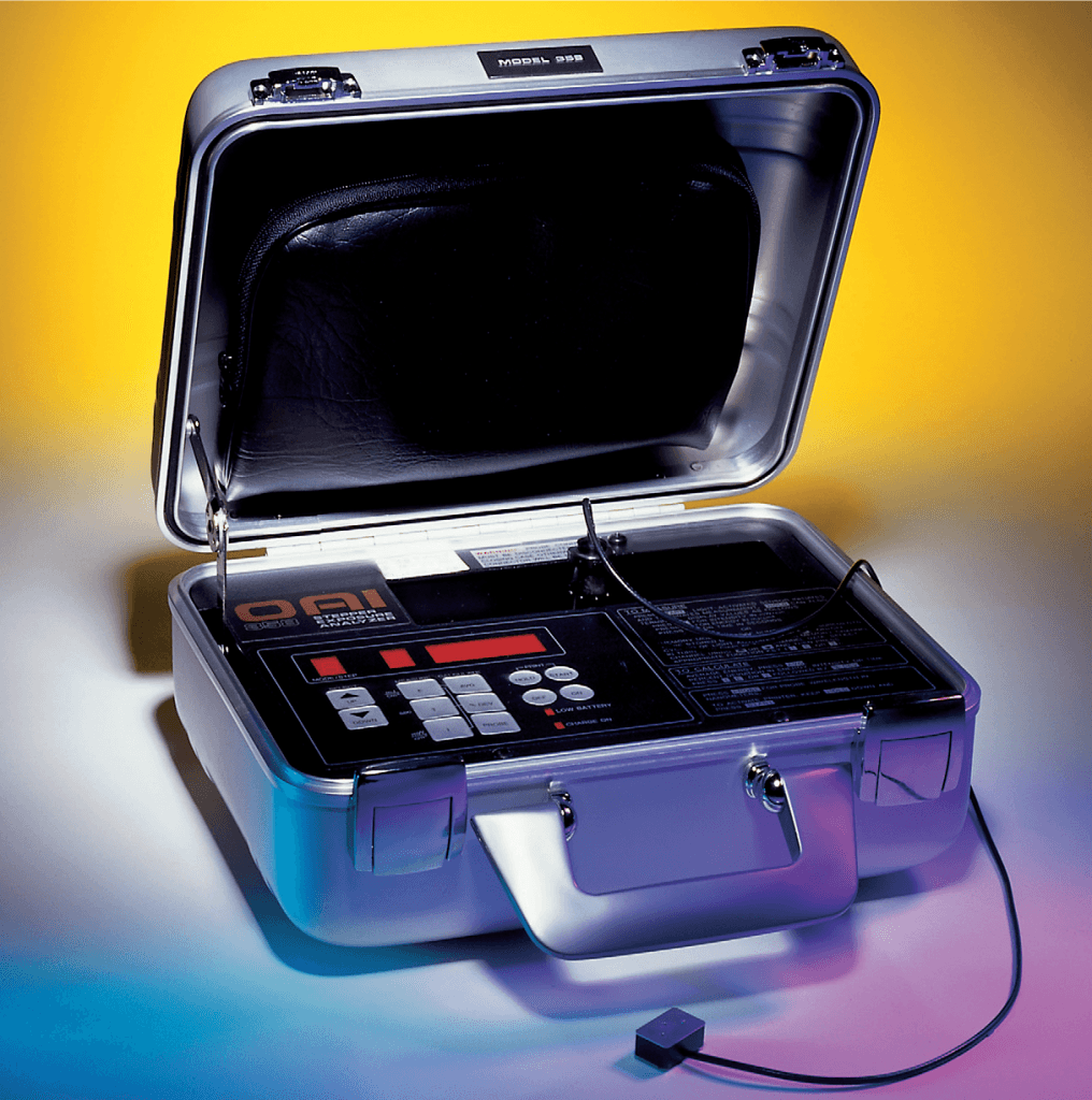
Perfect for a wide variety of industries where the precise measurement of UV energy is essential, the Model 356 is designed for any application requiring rep...
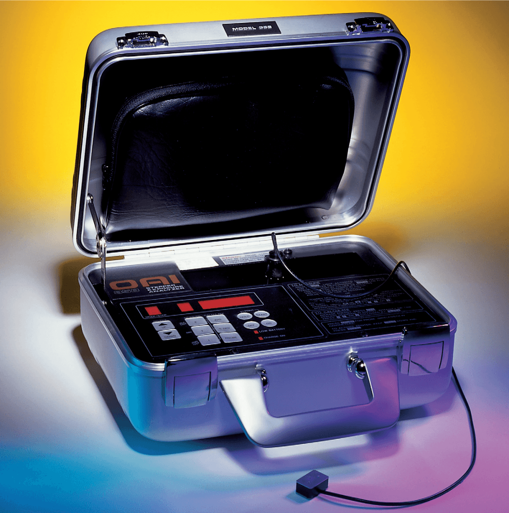
UV Intensity & Energy Meter。Designed for use with ASML, Canon, Nikon and GCA & Rudolph Technology Wafer Steppers the Model 457 UV Light Intensity & Energy Sy...
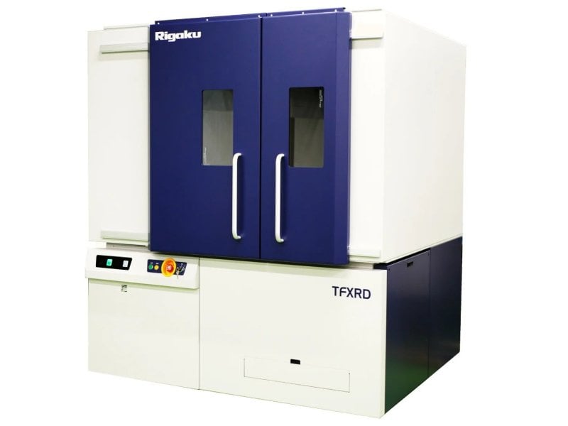
高分辨率X射线衍射(HRXRD)与X射线反射(XRR)系统,可实现非图案化外延薄膜的厚度、密度、表面/界面粗糙度、成分分布、应变、弛豫状态及倒易空间映射(RSM)的多维度表征。系统具备全晶圆映射能力,可覆盖直径达300mm的晶圆,适用于半导体制造的近厂(Near-Fab)应用场景。
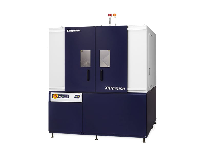
X射线形貌(XRT)成像系统,可针对功率电子、光电子及5G/6G通信领域的核心半导体材料(碳化硅(SiC)、氮化镓(GaN)、砷化镓(GaAs)、磷化铟(InP)、氧化镓(Ga₂O₃))开展单晶缺陷可视化表征,支持直径达300mm的晶圆测试。
.jpg)
一款新型全集成电子衍射仪,用于测量亚微米级晶体,支持从数据采集到晶体结构确定的体系化工作流程。产品线:Single Crystal、Electron Diffraction
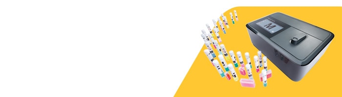
Spectroquant Prove 100 plus 面向主要使用 Spectroquant 测试套件或进行可见光测量的日常分析场景,属于 Prove plus 系列分光光度计。
 查看详情
查看详情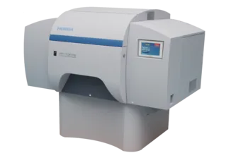
等离子体分析飞行时间质谱仪 (PP-TOFMS)可分析固体材料中化学成分随深度的分布,分析速度快,应用领域广, 是材料科学家理想的加工工具
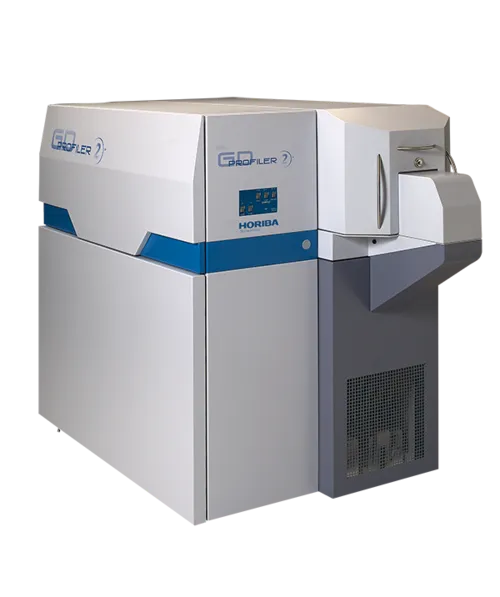
辉光放电光谱仪通过等离子体溅射,逐层剥蚀得到样品中各元素随深度的分布,元素的检测范围广,多种功能的开发帮助在不同的应用领域中都能发挥作用
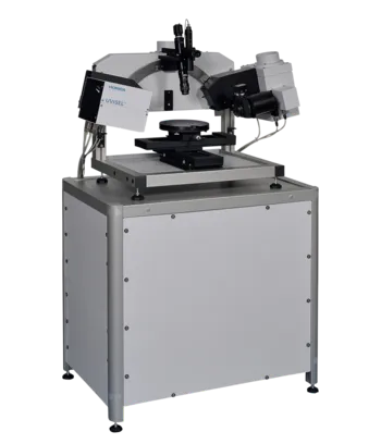
UVISEL Plus采用光弹调制晶体,测试过程中无任何移动部件,能够提供更好的稳定性和信噪比。光谱范围从190nm到2100nm。多种配置可供选择满足不同的需求。
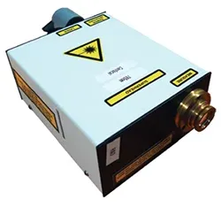
光纤耦合拉曼探头设计紧凑,坚固耐用,适用于多种应用,具有极高的灵活性。借助于可选配的集成摄像头,用户可以在拉曼分析之前精确定位感兴趣的区域。也可以采用浸入式探头和非接触式光学元件。

HORIBA 是完整测试方案的提供者,可以按照客户要求提供发动机、电机、传动系和动力总成测试台架的交钥匙解决方案。搭建交钥匙台架的一种可能情况是实现 HORIBA 测试设备集成在一个集装箱测试试验室。
 查看详情
查看详情 查看详情
查看详情第 35 / 37 页