INDIUM SERIES
INDIUM
Designed to Produce Precise Indium Bumps at a Longer Throw Distance for Flip Chip Applications
广西科米瑞实验仪器设备有限公司提供 Kurt J. Lesker INDIUM 产品资料、选型咨询、供货报价和售后服务支持,价格面议。
← 返回产品列表
说明
:Designed to Produce Precise Indium Bumps at a Longer Throw Distance for Flip Chip Applications
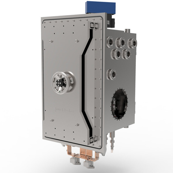
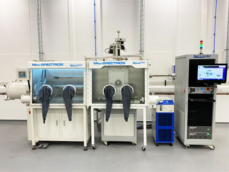
:The Kurt J. Lesker Company ® Indium series is a full-featured thin film deposition platform allowing depositions on wafers up to 200mm utilizing our advanced eKLipse control software. The INDIUM series is specifically designed for indium bump processing. A technically superior chamber design provides LN2 cooled substrates, thick indium depositions (up to 20µm), and extremely high deposition rates exceeding 100 Å/second. KJLC's eKLipse software control system allows stable rates, with long deposition runs allowing 10 wafers to be processed before breaking vacuum.
:Indium bump bonding is a technique used to create reliable and low-loss 3D flip-chip interconnects in superconducting circuits for quantum applications. Indium forms strong, stable bonds at room temperature that stay robust even at milli-Kelvin temperatures, due to its self-bonding ability and lack of brittleness at cryogenic levels. Its superconductivity at 3.4K also makes it ideal for low-loss quantum circuit bonds.
:Indium bumps can easily be fabricated in the Kurt J. Lesker INDIUM series physical vapor deposition (PVD) systems. Interested in creating indium bumps for your application? Then let's look at the key building blocks you will need for of an indium bump bond tool:
:The Kurt J. Lesker INDIUM series is an evaporation platform engineered and optimized for the fabrication of indium bump bonds. It offers user-friendly operation and streamlines maintenance, providing a reliable and versatile solution for this application.
:Long throw indium evaporation system.
:Large crucibles, indium slug feeder, and specialized shielding allow for multiple runs before venting the system.
:Features Available on INDIUM Series Systems
:Process Chamber
:The process chamber features an optimized geometry and size to promote excellent film uniformity and efficient material utilization. The source-to-substrate distance is set at a minimum of 15.5" (39.4 cm) to limit indium energy and reduce substrate heat load, while supporting high deposition rates exceeding 100 Å/sec (source and throw distance dependent). This configuration facilitates superior vertical growth of indium necessary for forming high aspect ratio bumps with robust lift-off characteristics. Cryogenic pumping maintains low base pressures, thereby reducing contamination risk and enabling rapid transition from atmospheric to process pressure.
:Indium Evaporation Sources
:Up to four high-capacity, shuttered thermal evaporation sources and KJLC material feeder facilitate the deposition of indium films up to 20 microns in thickness, with highly stable evaporation rates exceeding 100 Å/sec (source and throw distance dependent). This configuration ensures sufficient energy for the growth of indium bumps exhibiting high crystallinity and smooth surfaces with fine grain sizes.
:Due to indium's melting point of 157°C and evaporation temperatures exceeding 600°C, it is essential to shield critical components from exposure to liquid indium. Implementing water-cooling for the base flange and other vital parts enables stray indium to condense safely, minimizing the risk of electrical shorting during processing and ensuring optimal operational uptime.
:Source Protection
:Deposition shields and drip trays are used to maintain process uptime and simplify maintenance. The water-cooling system, combined with shielding, reduces the heat load caused by thermal evaporation and enables extended high-rate process runs of up to 3 hours per source.
:Indium Flux Monitoring
:Indium flux monitoring is achieved using fixed-position shuttered quartz crystal microbalances, ensuring precise rate measurement necessary for producing thick indium films. This system offers superior control over film thickness and deposition rates through the integration of KJLC's engineered eKLipse™ software and controls package. Consistent rate management and accurate film thickness termination facilitate repeatable and reliable processing.
:Substrate Fixture
:Multiple available substrate fixtures capable of operating at LN2 temperatures, or -30°C with rotating fixtures. Precision tilting and rotating fixtures are available to enable the formation of high aspect ratio indium films. Substrate cooling promotes out-of-plane indium growth, resulting in fine grain structures and smooth film surfaces ideal for bump bonding applications. Indium bumps can be deposited by employing substrate masks affixed to the fixture.
:The ion source, positioned either in a separate cooled chamber or within a isolated housing inside the process chamber, is safeguarded from indium contamination. Featuring a gridded design with an optional filament neutralizer, it effectively removes the oxide layer that forms on indium and can perform a light etch on the deposited metallic film. As a result, the indium film remains virtually free from contamination, ensuring optimal interfaces for bonding.
:Indium Metal
:Kurt J. Lesker Company offers high-purity indium metal in both pellet and wire forms, suitable for use in bump fabrication. The Kurt J. Lesker Company provides detailed indium evaporation guidelines and access to thin film process experts who are available to assist with technical inquiries related to indium bump fabrication.
规格
| 型号 | INDIUM |
|---|---|
| Product category | Thin Film Deposition System |
| 技术规格 1 | The Kurt J. Lesker INDIUM series is an evaporation platform engineered and optimized for the fabrication of indium bump bonds. It offers user-friendly operation and streamlines maintenance, providing a reliable and versatile solution for this app |
| 技术规格 2 | Long throw indium evaporation system. |
| 技术规格 3 | Process Chamber |
| 技术规格 4 | Indium Evaporation Sources |
| 技术规格 5 | Source Protection |
| 技术规格 6 | Substrate Fixture |
FAQ
相关产品


提交需求
请填写必填信息,我们将在工作日尽快回复。