TSV/TGV SERIES
TSV/TGV
Uniform, High-Rate Deposition for Complex TSV/TGV Structures.
广西科米瑞实验仪器设备有限公司提供 Kurt J. Lesker TSV/TGV 产品资料、选型咨询、供货报价和售后服务支持,价格面议。
← 返回产品列表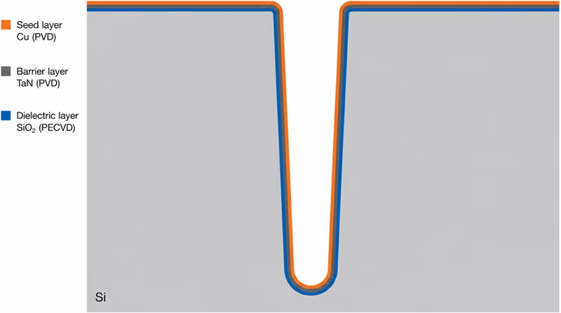
说明
:Uniform, High-Rate Deposition for Complex TSV/TGV Structures.
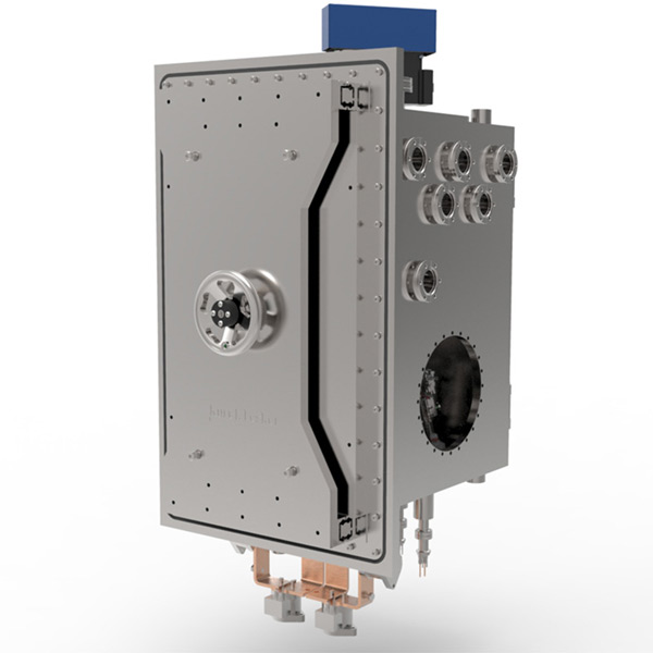
:The Kurt J. Lesker Company ® TSV/TGV Series specifically designed for depositions of Through Silicon Vias (TSVs) and Through Glass Vias (TGVs). A technically superior chamber design enables the deposition of adhesion, barrier and seed layers with high aspect ratio (up to 8:1) that are part of TSV and TGV architecture. KJLC's eKLipse software control system enables stable high deposition rates, with high uniformity, allowing 10 wafers to be processed before breaking vacuum.
:TSVs and TGVs are vertical electrical interconnects formed directly through silicon wafers or glass substrates to enable high-density, high-performance 3D packaging. TSVs are etched holes in silicon that are insulated, lined with barrier and seed metals, and then filled-typically with copper-to create low-resistance, high-speed connections between stacked chips or between a die and an interposer. TGVs serve a similar purpose but are formed in glass, which offers advantages such as low RF loss, excellent thermal stability, and smoother surfaces. Together, TSVs and TGVs provide compact, vertical signal paths that reduce wiring length, improve electrical performance, and enable advanced heterogeneous integration.
:TSVs and TGVs can be efficiently fabricated in TSV/TGV Series physical vapor deposition (PVD) systems. Interested in creating TSVs and TGVs for your application? Then let's look at the key building blocks you will need for of a TSV/TGV tool:
:Atomic Layer Deposition (ALD) for conformal coating into High Aspect Ratio (HAR) structures of > 10:1 such as used for TSV/TGV.
:Dual TSV system with a multi-substrate common load lock and robotic transfer. Shown transferring to a dedicated Nitride chamber with HiPIMS magnetron power supply and HiPIMS bias capability.
:High-aspect-ratio TSV with dielectric (non-PVD), PVD TaN barrier and Cu seed layer.
:Features Available on TSV/TGV SERIES Systems
:Application Driven Chamber Designs
:Single process chamber or dedicated process modules - each process chamber features an optimized geometry and size to promote excellent film uniformity and efficient material utilization.
:Substrate Stage
:Rotation heating or cooling available to improve film coverage and reduce voids. Heating of the substrate can assist in film densification, film adhesion and smoother morphology, while some applications benefit from cooling.
:Plasma/Ionization Options
:Alongside DC, pulsed-DC and RF options (material dependent) Kurt J Lesker is expert in the use of HiPIMS, a technique that creates a high level of metal ionization resulting in better sidewall step coverage at lower pressures. HiPIMS can also be added to the substrate for bias, which can increase side wall adhesion. OES (optical emission spectroscopy) is used to monitor plasma chemistry, particularly in reactive sputtering.
:Deposition Sources
:Full Face Erosion (FFE) KJLC TORUS MagKeeper sputter sources. Ideal for TSV and TGV deposition due to their magnetic design and high-density plasma generation provide excellent step coverage, uniformity, and low-damage deposition inside deep, high-aspect-ratio vias in silicon or glass, enabling reliable barrier and seed layers where conventional sputtering sources struggle. KJLC TORUS MagKeeper sputter sources enable quick and easy target exchange and operate at low process pressure, minimizing contamination and raising sputter deposition rates. Full target encapsulation shutters mitigate cross-contamination.
:Substrate Load Lock Options
:Single and multiple substrate options available. Dual chamber robotic transfer load lock shown, connected to a dedicated separate metals and nitride chamber.
:Typical Process:
:Load wafer loaded into the load lock
:Transfer into a pre-clean chamber for Ar ion etch
:Transfer to Metals chamber for Ti adhesion layer
相关产品


提交需求
请填写必填信息,我们将在工作日尽快回复。
